Summary of NNI at Ten: Nanotechnology Innovation Summit – Part 1
Posted on December 17th, 2010 | No Comments »
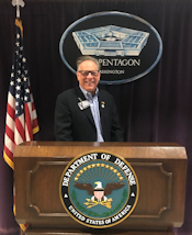
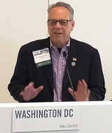
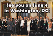
I enjoyed my time in DC at the National Nanotechnology at Ten: Nanotechnology Innovation Summit last week. I am very excited in regard to the next 10 years of Nanotechnology. Great to see our Nanotechnology Community friends such as:
Dr. Mike Roco, NSF; Doug Jamison, H&H; Peter Antoinette, Nanocomp; Piotr Grodzinski, NCI; Angela Belcher, MIT; Jeff Morse, National Nanomanufacturing Network; Kitu Bindra, Envia Systems; Alexei Andreev, H&H; George Allen, Former Senator of VA; Jim Mason, The ONI; Lynn Bergeson, B&C; Seth Coe-Sullivan, QD Vision; Travis Earles, White House OSTP; Charles Geraci, NIOSH; Bart Gordon, US House of Representatives, TN; Tom Kalil, White House OSTP; Terry Medley, Dupont; William Moffitt, Nanosphere; Matthew Nordan, Venrock; Mark Ratner, Northwestern University; Misti Ushio, H&H; Brent Segal, Lockheed Martin; Lloyd Whitman, NIST; Dave Arthur, SWeNT; Anita Balachandra, TechVision21; Craig Bandes, Pixelligent; Keith Blakely, NanoMech; Harry Bushong, nanoTox; Charlie Gause, Luna; Jim Hussey, NanoInk; Leonard Poveromo, Northrop Grumman; Chuck Van Fleet, Swan Chemical and Marlowe Epstein, NNCO
Here is a summary of the Nanotechnology Innovation Summit.
Last Thursday and Friday, December 9th & 10th, we attended the Nanotechnology Innovation Summit organized by our friends at NSTI on behalf of the agencies participating in the National Nanotechnology Initiative. The event, marking the 10th anniversary of the interagency Federal initiative, took place in National Harbor just south of Washington, DC. Attendees at a preliminary workshop held on Wednesday heard directly from program managers at numerous funding agencies, who described their research priorities in the context of the NNI Strategic Plan. As regular readers of this newsletter are aware a draft of the updated plan was posted on strategy.nano.gov for public comment throughout November. Since that plan calls for increased emphasis on goal-oriented research driven by national priorities, technology transfer, and support for commercialization activities, it is appropriate that “innovation” served as the theme for the anniversary workshop.
Travis Earles, Assistant Director of Nanotechnology in the White House Office of Science and Technology Policy, served as Master of Ceremonies for the Summit. You can read Travis’ own take on the proceedings (co-written with OSTP Deputy Director for Policy Tom Kalil) at the OSTP blog. Thursday opened with a keynote panel featuring a rare confluence of Presidential Science Advisors – Neil Lane (Clinton), John Marburger (Bush) and John Holdren (Obama) – giving a high-level Administration perspective. The Congressional point of view was presented by Bart Gordon, soon to retire as Representative from Tennessee and Chair of the House Science Committee, in Friday’s keynote address.
With Tom Kalil moderating, the Science Advisors (who also serve as OSTP Directors) each gave their perspective on the origins of the NNI and its course so far. Lane noted that what President Clinton liked to refer to as “my tiny little initiative” started in a time of budget surpluses and garnered rare bipartisan support. He is optimistic about the future of the initiative and remains convinced, as he told the House Science Committee when he was Director of the National Science Foundation, that nanoscale science and engineering is a key field for the future, but noted that we are headed for some tough budget years. Nevertheless the NNI’s budget growth from $495M in 2001 to an estimated $1.6B in 2011 is remarkable. Marburger noted that OSTP is lucky to have critical personnel just below the political appointee level who provide continuity across administrations. The success of the NNI through two presidential transitions is a testament to their value. He pointed out that we have known that interesting things happen at the nanoscale for a long time – that’s nature – but that the National Nanotechnology Initiative was founded to take advantage of emerging abilities to do something about it. The tools that enable this are high tech, but not particularly expensive, so the rise of nanotechnology programs around the world is not at all surprising. Marburger also noted that the planners of the NNI had paid attention to health, safety, and environmental issues from the very beginning, but that this has not been enough to satisfy the critics. He advocated for continued attention to the EHS issue, international competitiveness, and the difficulty of training skilled researchers and workers in a highly interdisciplinary field. Holdren expressed strong appreciation for his predecessor’s work in putting the NNI on solid footings, and listed five points that summarize the Obama Administration’s emphasis for the Initiative:
1. The NNI should continue to be a high priority for R&D agencies, as reflected in the annual Budget Memo he co-authors with the Director of the Office of Management and Budget, since nanotechnology is expected to play a vital role in economic growth and job creation.
2. Agencies should continue to support nanoscale science, engineering, and technology broadly but should increase activities supporting the NNI Signature Initiatives (to date, Nanotechnology for Solar Energy Collection and Conversion; Sustainable Nanomanufacturing – Creating the Industries of the Future; and Nanoelectronics for 2020 and Beyond, with the identification of new Signature Initiatives and establishment of supporting public-private partnerships called for in the draft Strategic Plan).
3. Nanotechnology research should support existing grand challenges in the research community, for example in sustainable energy or cancer therapeutics.
4. The emphasis on responsible development, as reflected by the growing funding for EHS research, will continue.
5. Concrete recommendations from PCAST for greater emphasis on innovation should be heeded through increased use of public-private partnerships and stronger technology transfer and commercialization efforts.
Following a break to explore the accompanying Innovation Showcase, leading figures from the business world discussed national and global issues driving the need for nanotechnology innovation. Norm Augustine, former Chairman and CEO of Lockheed Martin, noted that the “Gathering Storm” of international competitors identified in 2007 by a committee he chaired for the National Academies has not dissipated. In fact, a recent update to that report suggests we are losing ground. He noted that innovators do not respect boundaries, and that we continue to have a lot of good innovators in the United States, but fears that we are benefiting from our prior investments in educating scientists and engineers while falling behind in new investments. He urged us all to pay attention to how Congress treats the COMPETES Act in the next few years, closing with a quote from Winston Churchill: “You can always depend on Americans to do the right thing. After they’ve done everything else.” Jim Rudd of GE Global Research, while noting the many technological innovations GE has made based on discoveries here in the U.S., pointed out that the company now has 6 global centers in the research division, four of which are overseas (in China, Germany, India, and Brazil). GE does have over 100 research employees investing in nanoparticles, nanostructured materials, and coatings for applications like shedding ice from aircraft engines, improving heat transfer in steam turbines, and developing enhanced contrast agents for magnetic resonance imaging. Former Intel CEI Craig Barrett spoke about three main issues. He discussed the Nanoelectronics Research Initiative, perhaps the premiere example of an NNI-affiliated public private partnership, at some length. While recent generations of semiconductor electronics, from Intel and its competitors, include substantial amounts of evolutionary nanotechnology, the NRI is focused on revolutionary electronic devices and architectures to take the industry beyond the predicted end-of-life for CMOS technology, which he said is now expected to provide perhaps 12-15 more years of Moore’s Law improvements. On the policy side of things, Barrett echoed previous speakers concerns regarding education – he is now spearheading an effort called Change the Equation which is getting corporate America involved in STEM education. He pointed out that Intel’s venture capital arm, which he called the world’s biggest high tech VC supplier, used to make 90% of its investments in the U.S. That number is now down to about 50%, with the rest going to Asia. He also can’t imagine that the wafer fabs for future generations of semiconductors will be built in the U.S. much longer, given the substantial disincentives in tax and immigration policy relative to other countries.
The morning session closed with reports from three leaders of the nanotechnology investment community who are well known to NanoBusiness Alliance members – Harris and Harris’ Doug Jamison, Venrock’s Matthew Nordan, and Aymeric Sallin of NanoDimension. Doug outlined H&H’s long-term commitment to nano and microsystems technology, and discussed the firm’s pipeline of companies at various stages of maturity. He pointed out that the successes so far have come in extremely difficult times, with opportunities for exits all but non-existent for about five years. Doug noted the importance of partnerships for early-stage firms, both with larger, established companies and with research agencies. H&H has invested about $125M in their portfolio companies, which have attracted about $1.5 B in venture capital overall. While the $80M these companies have received in federal funds seems small in comparison, it is an important leveraging tool. Matt discussed investment in nanotechnology from his current perspective and in terms of his prior role as a founder of Lux Research. He pointed out the loss of 5.5 million U.S. manufacturing jobs over the last decade, and called science and technology innovation the only tool left in the U.S. competitiveness toolkit. While Venrock has a much broader focus than Lux – only Nanosys is an “obvious” nanocompany – other portfolio companies, for example several in the energy space, rely on nanomaterials and technology. Aymeric’s company invests exclusively in nano, and covers the field broadly. He claimed they screened 1700 companies in the past year, and took a more serious look at 173. Virtually all of their companies received NNI support in one form or another. Like H&H, their portfolio includes a mix of company maturities. As an example of a later stage company, he noted that Soladigm (which manufactures green building materials like switchable clear/tinted glass) is now hiring 300-400 people to ramp up their manufacturing.
Thursday afternoon featured two more technical sessions and another chance to visit companies displaying their wares at the Showcase. We heard from Northwestern University Professor and molecular electronics pioneer Mark Ratner, from IBM’s Tom Theis, and from Dawn Bonnell, Director of the Nano/Bio Interface Center at the University of Pennsylvania. Dr. Ratner pointed that nature’s solar energy conversion process, photosynthesis, utilizes aligned nanostructures and discussed synthetic analogues. He also discussed application in health care, especially diagnostics, and security. A long-time advocate for education and the development of young researchers, Mark pointed out that nanotech is still a young field, so it is especially important that we don’t just look to financials as a measure of success. We have real companies doing real things, and real students speaking the language. Quoting Thoreau, he concluded, “There is more day to dawn. The sun is but a morning star.” Dr. Theis discussed some of IBM’s most recent lab accomplishments in the realm of devices and systems for future generations of computers, including optical devices fabricated out of silicon and fully integrated with CMOS processing techniques and small, fast transistors made with carbon nanotubes or graphene. He noted that, despite their world-class research strengths, IBM can’t go it alone and relies on partnerships like the NRI to overcome the full set of barriers which must be overcome to deploy new technologies in the semiconductor industry. In addition to discussing why the “next switch” must not just be small but must be able to switch at lower voltages than scaled CMOS, he made an interesting remark about NSF’s new solicitation for proposals as part of the Nanoelectronics for 2020 and Beyond Signature Initiative. There are three eligible topics – new materials, new state variables, and new architectures or computing paradigms. Dr. Theis noted that by requiring proposals to address not just one of these topics but at least two, NSF was stimulating the kind of cross-disciplinary partnerships that are needed to identify manufacturable solutions from among the many things that physics allows. Dr. Bonnell was a participant in the “Nano2” study which we wrote about a few weeks ago, a broad survey of nano research in the U.S. and internationally. She noted that, while there is a lot of continuity in topics and programs since the start of the NNI, there are several current hot topics that were not foreseen. Two examples are graphene and nanoplasmonics. From her own Center’s work, she highlighted carbon nanotube-based sensors and cancer biomarkers. Finally, Dr. Bonnell noted that we must continue to evolve versions of our nano instruments that are capable of making measurements in manufacturing environments, as opposed to the research environments from which they generally come.
There were two more presentations from high-ranking Federal officials Thursday afternoon – Secretary of Energy Steven Chu, and Leo Christodoulou, Director of the Defense Sciences Office of DARPA. Secretary Chu summarized DOE’s plans to “Transform the Energy Landscape” before giving numerous examples of DOE-funded research into basic phenomena of importance for solar energy conversion, energy storage, efficient separation and capture of carbon dioxide or other greenhouse gases, and improved building technologies such as LED lighting. He discussed the Energy Innovation Hub program, sometimes called “Bell Lab-lets”, using the example of the Fuels from Sunlight Hub (Caltech/Lawrence Berkeley National Laboratory) with its ambitious goal of finding an artificial way to efficiently convert light and water to oxygen and hydrogen and then catalyze the production of a hydrocarbon fuel, mimicking photosynthesis but with much higher efficiency and an end product tailored to our fuel delivery systems. Dr. Chu concluded by saying that we have a lot of technologies in place as a result of research to date, but need new breakthroughs to meet our goals. Dr. Christodoulou spoke mostly about DARPA’s general approach to innovation – DARPA is not afraid to fail – although he noted that in briefing Deputy Director Ken Gabriel (who was originally scheduled to speak) for this meeting, he came up with plenty of impressive DARPA-funded “topdown’ nanotechnology. Examples include a tour-de-force maskless nanowriter, tip-based nanofabrication work, and functional interfaces. In contrast, he noted that the agency’s Blue Angel vaccine program is producing 16 million doses of vaccine per month, using tobacco as the bottom-up biofactory (a sort of surrogate nanowriter). He believes that if the 21st century is, as some have suggested, going to be the age of the control and manipulation of matter, more of our research will have to take high throughput bottom-up approaches.
Nanobusiness leaders rounded out the day in sessions devoted to innovations in energy technology, electronics, and manufacturing. A123 co-founder and MIT Professor Yet-Ming Chiang pointed out that batteries were probably not a significant factor in the initial NNI plans, but are now a big feature of the nano landscape. Transportation, storage of energy on the electrical grid, and consumer or industrial uses are all major application drivers of continued R&D. Dr. Chiang noted that his company initially intended to focus on another technology, but changed its course after observing fast full discharge behavior in some research cells. They’ve now built a business on the excellent discharge characteristics and cycle lifetimes of materials similar to those research cells, and continuing fundamental research promises further improvements. The company has some offshore manufacturing, but has invested heavily (with federal support) in new domestic facilities for production of both cells and battery packs. They now have over 700,000 square feet of factory space in Michigan. Four electric cars are using A123 batteries (the Fisker Karma, Hymotion plug-in converted Prius, and two vehicles built by Shanghai Automotive Industry Corp. for the domestic Chinese market). Navistar will soon deliver an all-electric delivery van for FedEx using their batteries, and A123-powered hybrid buses have already accumulated over 60,000 road miles. On the storage front, Southern California Edison will use A123 product in the world’s largest Lithium-Ion battery installation, at the Tehachapi Wind Project. Federal support has been very significant for the company, from its first DOE-SBIR grant through $100M of Automotive Battery Consortium funding and $240M of American Recovery and Reinvestment Act funds.
Seth Coe-Sullivan of QD Vision described his company’s two quantum-dot-based product lines: microdisplays, and LED lighting. Both were available for inspection at the Product Showcase, although the displays haven’t yet been released commercially. Since 22% of our nation’s electricity is used for lighting, and another 3% for displays, QD Vision’s approach has set out to decrease energy usage while improving performance. Their microdisplays are low power yet display a larger gamut of color than conventional phosphors, while their lighting products allow LED manufacturers to efficiently shift the spectrum of their emitters to provide perceived color quality comparable to traditional incandescent lamps. The Nexxus R30 LED lamp, which uses QD Vision’s technology, has a color temperature of 2700K and and outputs over 60 lumens per watt. The next-best available lamp with comparable color quality only put out about 40 lumens per watt. Seth discussed the importance of collaborating with established partners in your target industry. He also pointed out that his company is very committed to delivering nanotechnology safely throughout their products lifecycle, including disposal. They have worked with NIOSH, and are focusing research on lead- and cadmium-free quantum dots. As far as funding goes, QD Vision has received about two dollars in venture capital for every dollar of federal funding.
Damoder Reddy discussed Solexant and its ultrathin, roll-to-roll printed photovoltaic cells. The company, founded in 2006, has a small plant operating in the Bay Area and is constructing a 100MW capacity line in Oregon. Their work spun out of Dr. Paul Alivisatos’ group at Berkeley. While the current cells use Cadmium Telluride-bearing inks, they are developing a Cadmium-free version and hope to transition to that technology in about three years.
Brent Segal of Lockheed Martin Nanosystems described the fast, large, non-volatile memory technology originally developed at Nantero. Lockheed Martin bought the government systems division of Nantero a few years ago, with the original company focusing on commercial uses. Brent described the company’s “$31.5 Million journey” from an idea to a test board which flew on the Space Shuttle’s Hubble Repair Mission. Nantero’s success had an element of serendipity in it, since radiation hardness – considered a key feature for NASA and military applications – was not one of their original design goals. They continue to scale their chips, with a 64Mb generation coming soon and a 2Gb chip on the drawing boards. Brent is also an active participant in several nanotechnology standards development efforts, and he made a pitch for further participation in both standards development and public-private partnerships.
Peter Antoinette of Nanocomp Technologies says his company is delivering on the promise of scale. They are making carbon-nanotube-based yarns and sheets at a rate of several kilometers per week, while building next-generation facilities to further increase their output. The company has important partnerships with Rochester Institute of Technology and UMass-Lowell, and has worked closely with NIOSH and the EPA. Their CNT yarns have been incorporated into lightweight coaxial cables that are fully qualified for spaceflight, and their sheets have been used for EMI shielding on planes and satellites. One potential commercial application is in the entertainment wiring on the Boeing 7×7. Since this is a non-critical system, the qualification process is a relatively short 18 months or so. Peter noted that his is an intensely competitive field, with significant foreign competitors. So far, inflows of capital and talent have been sufficient to keep Nanocomp ahead.
S.V. Sreenivasan, Chief Technical Officer of Molecular Imprints and Professor at the University of Texas at Austin, described his company’s work in the memory and magnetic storage arenas. Beginning with DARPA funding in the mid-90s, they have developed lithographic processes with 1.5 nanometer critical dimension uniformity and 2.0 nanometer roughness control. A major application is in hard disk drives, where manufacturers will need patterned media within 18 months to stay on their continually improving capacity curve. MI’s 3rd generation of tools have the required specs, with the ability to create 15 nanometer pillars over large disks at a cost of ~ 35 cents per disk. They have also shipped a tool to an Asian NRAM manufacturer which can process ten 300 millimeter wafers per hour, for use in memory chips with feature sizes < 25 nanometers.
Dr. Angela Belcher was the final speaker on Thursday. As many of you know, in addition to serving as Germehausen Professor of Materials Science and Engineering and Biological Engineering at MIT, Angie is a co-founder of not one but two nanotech companies – Cambrios Technologies and Siluria. Dr. Belcher discussed these companies’ work to commercialize her research on biomaterials, virus-guided self-assembly, etc, but her most telling remark may have been this: the beginning of NNI coincides pretty directly with the beginning of her research career. She never knew a research landscape without an NNI, and finds it difficult to imagine. Dr. Belcher is truly one of the first of those new-generation innovative interdisciplinary thinkers that earlier speakers pointed to as among the most valuable products of the Initiative. With that thought, we’ll close for today. A discussion of the Friday activities at the Nanotechnology Innovation Summit will be forthcoming. In ten years, there has truly been a lot of progress to cover!
Last week’s conference was fabulous. If you have any additional questions, please feel free to contact me at vincentcaprio@nynanobusiness.org.
Regards,
Vincent Caprio “Serving the Nanotechnology Community for Over a Decade”
Executive Director
NanoBusiness Alliance
203-733-1949
vincentcaprio@nynanobusiness.org
www.nanobusiness2010.com
www.vincentcaprio.org


