NanoBCA Interview: Greg Schmergel, Co-founder, Chairman & CEO, Nantero, Inc
Posted on March 12th, 2019 in Uncategorized | No Comments »
The NanoBusiness Commercialization Association (NanoBCA) is excited to announce the return of our NanoBCA Interview Series. Through this series we offer in-depth interviews with some of the key stakeholders influencing our nanotechnology community today. Many of these dynamic professionals will be participants at our:
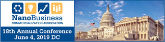
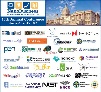
18th Annual NanoBusiness Conference
Tuesday, June 4, 2019
K&L Gates Washington DC
This month the NanoBCA is pleased to share the following interview with Greg Schmergel, Co-founder, Chairman and CEO of Nantero Inc.
Steve Waite: Thanks for taking the time to speak with us today, Greg. We are coming up on a major milestone for Nantero later this year. Tell us about it.
Greg Schmergel: Yes, that’s right. Fujitsu announced that they will be bringing NRAM to market in late 2019 so it looks like they will indeed be the first to market with an NRAM product. We are very excited about that especially because Fujitsu is a very experienced company with bringing new memories to market. They brought FRAM to market many years ago and have sold very high volumes of it. They probably have the most experience of any company in the world at bringing a new memory to market. Certainly, in terms of number of units shipped of a memory that isn’t DRAM or Flash, the two mainstream memories. They are a great partner for Nantero.
SW: That is all very exciting, indeed. What are Fujitsu’s initial target applications for NRAM?
GS: Fujitsu plans to use NRAM for a wide variety of applications and sell it to their customers who will also use it for a wide variety of applications. It will take a couple of years to ramp up to high volumes, but that is the direction things are moving in today.
SW: Sounds like Nantero will begin to see meaningful top line growth in the years ahead as Fujitsu’s NRAM commercialization efforts ramp up.
GS: Yes. I would clarify that we have already brought in substantial revenue, in excess of$80 million cumulatively, from license fees and engineering fees. Nantero is not a pre-revenue company. But in terms of royalty revenue from products, yes, that’s when it will start. Overall, what is happening with Fujitsu this year is a huge milestone for us, and for the field of carbon nanotubes (CNT) in general. It is a field that has had a tremendous amount of promise for a long time. We made the transition years ago from the laboratory to fab and started developing this product in the fab. And now the next step is to transition from the fab into the customer’s hands. We are very close to that milestone.
SW: It is noteworthy that Fujitsu is leading the charge on CNT memory devices, given that CNTs were discovered in Japan back in the early 1990s.
GS: That’s correct. It makes sense and is very appropriate that the first CNT memories would come out of Japan.
SW: Tell us about the major benefits of Nantero’s CNT-based NRAM versus conventional non-volatile memory devices.
GS: Compared to Flash, which is the dominant non-volatile memory in the market today, NRAM has far higher performance. The performance of NRAM is actually more DRAM-like, both in terms of speed and endurance, so you get much, much better performance. Compared to DRAM, NRAM is non-volatile whereas DRAM is volatile. While you have similar performance to DRAM, you get the non-volatility of Flash, which dramatically reduces your power consumption. On top of that, we can achieve lower price per bit for the customer than DRAM, as well as higher densities.
As you know, just about every memory application out there is now hungry for more memory storage. Every trend out there – Big Data, Cloud Storage, AR, VR – all demand more and more memory. Providing more, fast memory at a lower cost per bit is something very valuable for a whole range of applications. Depending on what type of device you are putting NRAM into you get substantial speed increases, reductions in power consumption and also higher robustness.
For example, Schlumberger invested in us because they wanted a memory that would survive under high temperatures. Lockheed Martin purchased our government business unit in part because of the ability of our memory to survive under heat, radiation and vibration. That was demonstrated in the launch of our memory on the Space ShuttleAtlantis and its excellent performance through the whole mission, despite the high radiation in space.
Depending on the application, there are a lot of major benefits of NRAM. And, of course, if you own a data center, our memory is extremely valuable to help reduce and deal with the problems of heat generation and power consumption that data centers struggle with, in addition to making them faster so they can handle more transactions or searches or whatever the datacenter is handling.
SW: You highlighted a few application areas of NRAM. It would seem as though a great deal of the emerging technology areas such AI, IoT, 5G and Blockchain-based applications would all benefit from NRAM. Is that correct?
GS: That is absolutely right. All of these trends accelerate and accentuate the demand for more and more memory, and for more, fast memory, as well as for lowering power consumption. Power consumption is actually one of the biggest issues facing just about every category in the electronics industry. Data centers are consuming a measurable percentage of the world’s power now. For AI, trying to make something perform like a brain but doing that without exceeding the heat tolerances and melting the system is a challenge. It is not a problem with brains, but with chips it is a problem.
With smartphones, of course, power consumption which ties to the battery life is one of the major issues. As you add more and more features, like AR and VR, you start to eat up the battery faster and faster. Consumers today expect ten hours or so of battery life. If you are selling a smartphone with only three hours of battery life nobody wants it anymore, even if it has lots of cool features. We need to find a way to incorporate all of these new features into a phone while maintaining the same or hopefully even a longer battery life.
SW: Given the major benefits of NRAM, I would imagine that you are seeing greater interest these days from large, established companies who are investing heavily in these emerging technologies?
GS: Yes. Fujitsu Semiconductor is planning its own product family for NRAM that will target a host of applications. And Fujitsu Foundry, which is the manufacturing part, can run both designs made by Fujitsu Semiconductor, but also designs made by Nantero as well as designs made by other customers. The fact that the manufacturing process for NRAM is available at Fujitsu Foundry will support a wide range of customers and designs.
SW: Are there other foundries interested in NRAM?
GS: Yes, there is absolutely interest from other foundries. We are talking to other foundries and are engaged with other foundries, but we can’t talk publicly about this activity at the present time.
SW: Nantero has patented a fabrication process involving CNTs and conventional semiconductor fabrication equipment. That intellectual property seems valuable in this day and age.
GS: Yes, exactly. Fabs do not need to buy new types of equipment that they have never bought before. They can use the same types of equipment that they buy from their current vendors, so there is no need for any special type of CNT equipment.
I would also point out that CNTs add tremendous value for devices that are made at larger nodes than the 7 nm level that is posing a challenge for some foundries today. For example, our memory technology can be stacked in multiple layers in the same die. At older nodes greater than 7 nm, we can achieve higher and higher densities of memory. Those older nodes can be utilized, while adding additional value for customers. It is true that only a very small number of fabs can scale silicon processes beyond the 7 nm level. But there is still a huge amount of fab capacity above 7 nm, and new materials such as CNTs can help continue to increase value for customers at those nodes in coming years.
SW: How does the competitive landscape look for Nantero at the present time?
GS: The competitive landscape is pretty broad because Nantero’s NRAM is suited for both standalone memory as well as embedded memory, and for both low and high- density memory. For example, we have already done a multi-gigabyte product design for one customer. For some companies like Fujitsu they have announced that their products will be in the megabits range, up to very high megabits. For other customers, they want products in the gigabit or even gigabyte range, and we are supporting them on that as well.
NRAM can operate across a wide range of densities. I think the key is that, as far as we know, there is only one memory device – Nantero’s NRAM – that has both non-volatility and DRAM-like speed and performance while being at a lower price per bit. That is a unique combination and value proposition for customers, whether they are used it for embedded memory or as a standalone memory. What’s exciting is that NRAM can enable new devices that were not possible before with today’s memory.
SW: That is exciting.
GS: It is, indeed. I think the analogous situation you can look to is Flash memory. When Flash was introduced in the 1980s it offered the feature of non-volatility which DRAM did not offer, and then people figured out that they could make a smartphone and they can make an SSD using that feature. And those were very exciting and influential products that could not be made practically without Flash memory. And similarly, with NRAM memory we think there are a lot of exciting, new products that people can come up with that just would not be practical otherwise.
SW: I know Nantero has been focused on NRAM, but there is also a role for CNTs in microprocessors, GPUs and the like? Do you see an opportunity to leverage Nantero’s expertise beyond NRAM into other types of devices?
GS: Yes, we do. There are a lot of applications in addition to CNT memory. In fact, because we had to become the first company in the world to get CNTs into mass production CMOS fabs, in order to make our memory, that forms the foundation to use CNTs to mass produce, in a CMOS fab, any other CNT device. For example, CNT transistors, CNT sensors, CNT interconnects. The mass production of all of these devices can be enabled with our intellectual property as well. We have 185 patents granted in the U.S. alone and more around the world, as well as more pending. We do have a very large and consequential and I believe unrivaled IP portfolio in the CNT electronics space. And those other applications are quite exciting for the future.
SW: You have spent a lot of time in Silicon Valley as well as Asia. What are the major differences you see between the regions in terms of investor interest in Nantero?
GS: There is a lot of interest in Silicon Valley but even more in Asia where there is a lot more recognition of the value of semiconductors as the foundation of the electronics industry and much more willingness to invest in it. Additionally, investors in Asia have a longer time horizon. Developing a chip is not a one or two-year project. It is a long-term project. Especially developing a new memory chip, which is one of the most complex and difficult pursuits you can undertake. As evidenced by the fact that there have been only two mass production memory chips developed in the last 80 years – DRAM, which was invented in the 1960s, and then Flash in the 1980s.
Developing a new memory chip is an event that happens only once every few human generations. In Asia, they do have a longer-term perspective. We have spent a lot of time there building up relationships and view that as a critical region for Nantero. Unfortunately, in Silicon Valley, it is often harder to find those types of perspectives.
SW: Silicon Valley seems to have migrated away from investing in silicon, which seems a bit ironic.
GS: Exactly. The number of investors in Silicon Valley investing in silicon is getting closer to zero than one would like to see.
SW: At a time when we appear to be hitting a wall with silicon at sub-7 nm levels.
GS: Right.
SW: The commercialization of NRAM has been a long time coming – almost two decades. What are some of the major lessons you have learned as an entrepreneur working with an emerging nanotechnology?
GS: Well, for starters, it hasn’t been an easy sell with investors. It requires a tremendous amount of persistence. In terms of lessons learned, the sooner and more deeply integrated you can get with the end customer the better, so that everything you do is driven by the needs of the end customer. That is opposed to just developing a technology in a vacuum.
Similarly, the sooner you can get can get integrated with the mass production facility that you would like to use, the better. We did some work in the laboratory early on and then later on had to rethink all of that work once we got into a mass production fab. Overall, the sooner you can get into the mass production facility, learn what the rules and requirements are for mass producing the device, the better.
SW: Nantero has a number of prominent strategic investors. What can you tell us about them?
GS: Nantero has worked hard to bring on numerous strategic investors over the years. We have nine strategic investors currently, only four of which we are allowed to disclose at the present time. Those four are Schlumberger, Dell, Cisco and Kingston.
SW: That’s a pretty distinguished group. Given where Nantero is right now on the verge of hitting a major milestone, what are company’s current needs? Are you still open to new investors, strategic and otherwise?
GS: Yes, we are. Investors interested in Nantero can feel free to contact me. I would be happy to talk with them.
SW: Very good. One last question for you today, Greg. Nantero has a licensing model similar to ARM Holdings, PLC, which was acquired by Softbank for over $30 billion a couple of years ago. When you look out over the next several years, do you see an opportunity for Nantero to go public as commercial revenues begin to ramp?
GS: Sure. That is a possibility. We could certainly envision following a path similar to ARM and doing an IPO.
SW: Well, that certainly would be an event worthy of celebration by all in the nanotechnology community. We all know how hard you and your team have worked over the past eighteen years. Thanks again for your time, Greg. We wish you and Nantero all the best in the future.
For more information about Nantero, visit nantero.com.

Steve Waite is a member of the NanoBCA Advisory Board and author of several books including Quantum Investing and Venture Investing in Science.
I hope you enjoyed this month’s interview. Looking forward to seeing you on June 4th in DC!